Modeling, Modulation Analysis of Filter-Integrated Three-Switch Boost Inverter
7/25/2024 2:23:33 PM
| Topics covered in this article: |
| Ⅰ. Introduction to Distributed Generation System |
| Ⅱ. Modeling And Modulation Analysis Of The TSBI |
| Ⅲ. Summarizing with Key Points |
Ⅰ. Introduction to Distributed Generation System
With fossil fuels running out, distributed power generation systems (DGs) have gotten a lot of attention for being good for the environment. Inverters are very important to the energy conversion process because they are the link between the loads and the DGs. Voltage-source inverters (VSIs) and current-source inverters (CSIs) are the two types of inverters based on the type of power supply on the DC side. Since CSI needs a big inductor in series on the DC side, which will make the system bigger, VSI is used more often in real-world situations.
But active switches and some other devices will cause the output current to have a lot of harmonics. If there are too many harmonics, the system's loss will go up, and the circuit may stop working. Therefore, putting in a filter to get rid of the harmonics is needed. LCL filters and L filters are the most common types of devices used today. Compared to L filters, LCL filters need less space and have better harmonic suppression for high-frequency signals. But the LCL filter has a big drawback that makes it less useful.
LCL filters' bode diagram has a clear resonance peak at the resonance frequency, which can easily lead to system instability. So, to stop the resonance spikes, both active and passive damping methods have been suggested. With the passive damping method, resonance spikes are suppressed by adding resistors to the circuit. With the active damping method, the damping function is achieved by changing the control algorithm so that it does not cause additional loss to the system.
Similar to the active damping method, implementing the filter function in the three-switch boost inverter (TSBI) does not need any extra resistors. It stops resonance spikes by controlling the switches in the TSBI network. Also, since VSI is a buck inverter, its output voltage is lower than the DC voltage. A boost device needs to be added to the system to make sure that the inverter's output voltage can meet the needs of the equipment. At the moment, the most commonly used method is to add a boost converter to the DC side.
Z-source inverter (ZSI) and the quasi-Z-source inverter (qZSI), which are two new types of high gain converters previously introduced. But putting the boost device on the DC side will increase the voltage stresses on the switches in the H-bridge circuit. When the switch is under a lot of voltage stress, the system's stability suffers. So, the user can choose expensive high-voltage switches that can last a long time, which will make the system cost more.
Based on the LCL filter, the TSBI is made by adding a filter capacitor and three bidirectional switches. Compared to ZSI and qZSI, the voltage stress on the switches is reduced. By controlling the switches in the TSBI network, the filter function, the boost function, and the system's resonance spike can also be significantly dampened.
Ⅱ. Modeling And Modulation Analysis Of The TSBI
Topology of the TSBI
As shown in Fig. 1, the integrated circuit is made up of three bidirectional switches, two filter capacitors, and two filter inductors. One pair of complementary signals can control all three switches. The control signals for switches K1 and K3 are the same, and the control signal for switch K2 is the opposite of the control signal for switch K1. The structure of the TSBI network changes when the gate signal changes. Fig. 1 shows that there are three vector states for the TSBI: the active vector state, the boost zero vector state, and the traditional zero vector state.

Fig. 1. The topology of TSBI. Source: IET Power Electronics
Active vector operation state
Fig. 2 shows that switches K1, K3, are ON, switch K2is OFF, and a capacitor C1 is inserted into the circuit in the form of a parallel capacitor C2. Using the Kirchhoff voltage law (KVL) and the Kirchhoff current law (KCL), the following equations are established for the time interval when the system is in the active vector state T0 .


Fig. 2. Flow path in an active vector state. Source: IET Power Electronics
where p = d/dt, RL1 is the stray resistance of the inductor L1; RC1 is the stray resistance of the capacitor C1, iL1 is the current of the inductor L1, iL2is the current through the inductor L2, uC1 is the voltage of the capacitor C1, uC2is the voltage of the capacitor C2, ui is the output voltage of the H-bridge and uo is the voltage of the load.
Boost zero vector operation state
In the boost zero vector state, the switches K1, K3 are OFF, the switch K2 is ON. As shown in Fig. 3, the switches S1 and S2 (or the switches S3 and S4) in the H-bridge are ON, and the output voltage of the H-bridge is 0. Assuming the time interval when the system operates in boost zero vector state is T1, the following equations can be obtained.

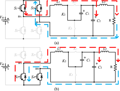
Fig. 3. Flow path in the boost zero vector state. Source: IET Power Electronics
Traditional zero vector operation state
In the traditional zero vector state, the switches K1 and K3 are both ON, the switch K2 is OFF. As shown in Fig. 4, the switches S1 and S2 (or the switches S3 and S4) in the H-bridge are ON, and the output voltage of the inverter bridges is 0. Assuming the time interval in this state is T2, the following equations can be obtained.


Fig. 4. Flow path in the traditional zero vector state. Source: IET Power Electronics
Boost factor analysis
According to the voltage-second balance principle, when a system is in a steady state, the average voltage of the inductor is 0.
For one switching cycle TS, the time interval of the boost states is T1, D =T1/Tswhich gives the system's boost duty cycle. From equations (1–12), the following equation can be obtained:

where x, y1 and y2 can be expressed as (14).

The relationship between the voltage of the capacitor-C2 uC2and the input voltage ui is as follows:

In the same way, according to the principle of ampere-second balance, when the system is working at steady state, the average value of the capacitor current is 0. So, the following equation is obtained.

The relationship between the current of the load iR and the current of the inductor-L1 iL1 is

Under the condition of considering only the resistance of the capacitor C1 and the load resistance R, assuming ratio = rC1/R, the curve of boost factor versus D with different ratios can be obtained as shown in Fig. 5.

Fig. 5. Gain comparison of the TSBI with different rC1/R. Source: IET Power Electronics
The relationship between the voltage uC2and the inverter output voltage ui can be expressed as follows in the ideal case (rL1 = rL2 = rC1 = rC2= 0).

and the voltage gain G of the system can be expressed as:

where M is the modulation index of the inverter. Fig. 6 shows the G versus the D and M of the inverter.

Fig. 6. Voltage gain G versus D and M of the inverter. Source: IET Power Electronics
PWM modulation strategy
According to the above analysis, the working modes of the system are sorted out as shown in Table 1.
Fig. 7 shows the PWM control method. The gate signals of switch S1 and switch S3are obtained by comparing Vm with Vtri, and the gate signals of switch S2and switch S4 are obtained by comparing -Vm with Vtri.
Table 1. Switching combinations, vector states, and inverter output voltage


Fig. 7. Generation of the PWM control signals. Source: IET Power Electronics
As shown in Fig. 8, the gate signals of switches K1, K2and K3 are obtained by comparing the reference of the duty cycle (1-D) with the triangular carrier Vtri.
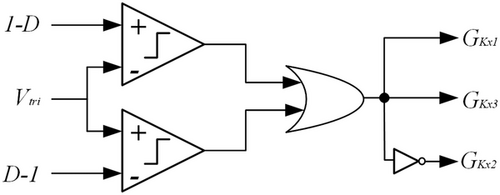
Fig. 8. Logical diagram of switches' control signals. Source: IET Power Electronics
Ⅲ. Summarizing with Key Points
Some of the takeaways from the article are as follows:
The article provides valuable insights into the modeling and modulation analysis of a filter-integrated three-switch boost inverter, which is an important component of distributed power generation systems.
The article highlights the importance of inverters in energy conversion and explains the two types of inverters based on the power supply on the DC side.
The article also emphasizes the need for filters to eliminate harmonics that can cause system loss and circuit failure, which is crucial for ensuring the reliability and efficiency of power generation systems.
The TSBI topology analysis presented in the article provides a detailed understanding of its three vector states, which can help engineers design more efficient and reliable power generation systems.
Overall, this article is a valuable resource for researchers, engineers, and anyone interested in understanding the principles behind filter-integrated three-switch boost inverters and their role in energy conversion.
This blog post is part of a full research article from IET Power Electronics.
The featured image is courtesy of Midjourney.
Latest Products
-
AD9834BRUZ
Analog Devices Inc.
-
BAV99W,135
Nexperia USA Inc.
-
IP5002CX8/P135
NXP USA Inc.
-
ADAU7002ACBZ-RL
Analog Devices Inc.
-
PGA2320IDW
Texas Instruments

-
SRC4184IPAG
Texas Instruments
-
MUSES72320V-TE2
Nisshinbo Micro Devices Inc.
-
PCM2706CPJT
Texas Instruments
 Upload BOM

